How technical decisions shape the outcome of patent litigation in semiconductors, new energy technologies and advanced materials
Three technical pressure points, the evidentiary “funnel” and the “squeeze effect” in UPC practice — including an in-depth analysis of the UPC case Seoul Semiconductor v. Expert eCommerce
Disclaimer: This article is provided for general information only and does not constitute legal advice in relation to any specific case.
Introduction
The speed of proceedings before the Unified Patent Court (UPC) is not merely a matter of timing. It is a structural feature of the system: technical issues, claim construction, evidence and fallback positions are all brought forward to an early stage of the proceedings. In semiconductor, new energy and advanced materials cases, this structure gives technical issues exceptional importance. The technical interpretation adopted at the outset will often determine whether evidence can be obtained, whether it can be understood by the court, and whether infringement and validity can be argued coherently within the same technical narrative.
This article uses a transferable methodology to address a fundamental point: in semiconductor patent litigation, the legal outcome often depends on three technical pressure points: claim construction, the technical evidence path and the early identification of invalidity risks.
1 | Why the technical route often matters more than legal wording in the UPC era
Patent disputes in the fields of semiconductors, new energy technologies and advanced materials are usually not decided by a simple comparison of words. They typically turn on a chain of technical issues: device structure, process implementation, material properties and functional effect.
The UPC’s front-loaded procedural structure further requires these technical chains to be presented in a structured way at an early stage. If the technical interpretation is unclear, if the evidentiary path is incomplete, or if invalidity risks are not fully identified, the room for later correction becomes significantly narrower.
2 | Three pressure points: construction, evidence, invalidity — and the underlying squeeze effect
Pressure point 1: Claim construction
In semiconductor, new energy and advanced materials cases, claim construction is highly dependent on the microscopic morphology of materials, process features and device structures. Structural language and functional language together determine the scope of protection. In other words: the technical context determines the legal context.
Pressure point 2: The technical evidence path
In complex semiconductor cases, particularly before the UPC, the question of whether an accused product has a particular infringing feature often comes down to three questions:
- Can the feature be reliably detected?
- Can the result be understood by the court?
- Can the defendant’s counter-arguments be excluded or at least addressed?
This leads directly to the idea of an evidentiary “funnel”: material characterisation results must be translated into a chain of legal facts that can be accepted by the court.
This point is important because the UPC procedural framework places clear demands on factual allegations and evidence. A party relying on facts must provide evidentiary support for factual assertions that are contested or likely to be contested.
Pressure point 3: Identifying invalidity risks
In semiconductor cases, the real risk posed by the prior art often lies in the functional implementation path, not in a superficial similarity of terminology. In European practice, the decisive lever in the assessment of inventive step is frequently technical motivation.
The fourth underlying risk: the squeeze effect in parallel proceedings
Where validity and infringement proceedings, or UPC and EPO or national proceedings, run in parallel, a narrow interpretation adopted to avoid a prior-art attack may later allow the accused embodiment to escape infringement. The same is true in the opposite direction. A broad interpretation may help on infringement but increase validity risk. This is the squeeze effect.
3 | Claim construction is not a purely legal exercise — the technical context defines the legal boundary
In UPC practice, claim construction is shaped by two general principles and two important limitations.
The patent specification is its own dictionary. However, the description cannot be used in a way that contradicts the claims. For example, subject matter deleted from the claims during prosecution but still present in the description cannot simply be reintroduced through claim construction. In addition, definitions of self-created technical terms that are not commonly used in the relevant industry are relevant only for interpreting the specific technical feature to which the definition relates.
Claim construction must be carried out from the perspective of the skilled person. In semiconductor and advanced materials cases, this perspective is highly dependent on the relevant materials, including not only their composition but also their microstructure, as well as on processes and device structures, such as layer thicknesses and stacking arrangements.
Practical point: If, at the claim construction stage, the case is framed around the idea that “the name of a layer equals its legal identity”, the evidence will naturally be directed towards proving that the other side’s naming is incorrect. In semiconductor and advanced materials cases, this is often inefficient and sometimes dangerous.
The better approach is usually to return to function and material properties, and to build a chain of proof based on suitability and effect.
4 | Designing the evidence path — “visible” does not mean “legally established”
4.1 Three operational questions: detectability, comprehensibility and resistance to challenge
The question of whether an infringing feature is present should be broken down into three operational questions: can it be detected, can it be understood, and can it withstand challenge?
For a litigation team, this means that the evidence path must be designed. Sampling, preparation, test methods, parameters, presentation and explanatory logic must all be reproducible and defensible.
Material characterisation results are not the end point. They are not even necessarily the legal fact itself. They are the starting point of the evidence chain. What the court needs is a legal fact that is verifiable, explainable and capable of withstanding challenge.
4.2 Characterisation is only the starting point: TEM, EDX and SIMS merely indicate structure
Images and elemental distributions are not conclusions in themselves. Expert explanation is required to show which interfaces form a “layer”, which gradients are attributable to interdiffusion, and which thicknesses correspond to a particular function. The court needs an explanatory chain: image, explanation and mapping to the claim language.
4.3 An engineering standard for evidentiary sufficiency before the UPC
The UPC’s approach to evidence can be condensed into the following practical standard:
Evidentiary sufficiency = representativeness + repeatability + explainability.
This may require multi-point sampling, verification across multiple chips, a clearly defined preparation procedure and measures to exclude the argument that the sample is not representative.
Practical point: Evidence engineering must be reproducible. It is not enough that the test can be performed. The evidence path should be designed so that the opposing expert cannot reach the opposite conclusion using the same route, or must at least explain why such a different result is obtained.
4.4 Claim construction is the technical blueprint for measurement and evidence collection
Claim construction must come first because it defines the measurement target and anticipates possible defence strategies. If testing is carried out first and the interpretation is added later, the evidence may fail to address the relevant claim features.
The technical blueprint must be drawn before the testing begins. Otherwise, the more precise the measurement becomes, the greater the risk that it moves away from the legal requirements.
Practical point: Many cases are not lost because there is no evidence. They are lost because the evidence is not aligned with the claim features. Alignment with the claim features takes place during claim construction and the development of the testing strategy, not during the later processing of test data.
5 | Identifying invalidity risks — functional implementation path and technical motivation
In semiconductor cases, the risk posed by prior art arises from the functional route, not from superficial similarity in terminology. The depth of technical understanding determines the assessment of novelty and inventive step.
In engineering practice, the same structure may be described using different terms, especially across companies, disciplines and process nodes. Conversely, the same term may refer to different structures. Terms such as “extension layer” or “barrier layer” may have different meanings in different technical systems.
This reflects how knowledge spreads in materials and device technologies. Many key technical points exist in the form of engineering experience or parameter windows. Their textual expression is naturally unstable.
The real question for novelty and obviousness is often whether the function and the underlying physical mechanism are structurally and technically equivalent. If an invalidity search and comparison rely too heavily on identical terminology, genuinely high-risk documents may be missed.
In European and UPC practice, inventive-step analysis often turns on technical motivation. If the prior art does not disclose the problem addressed by the patent, or if the thermal matching of existing materials or structures means that there is no reason to add a further functional layer, the mere addition of a layer is not necessarily obvious.
Practical point: Invalidity disputes are not a comparison of material lists. They are a confrontation between technical narratives based on problem, mechanism and motivation. The litigation team must explain the causal chain of materials science and device physics in order to build an effective defence on inventive step.
6 | How the UPC’s front-loaded procedure amplifies these issues — and how the squeeze effect arises
The key connections in semiconductor and advanced materials litigation can be summarised as follows:
- early identification of disputed issues;
- claim construction as the technical blueprint for evidence collection;
- early technical analysis, including functional reasoning, before testing and evidence collection;
- structured evidence paths, from factual evidence to legal conclusion;
- invalidity risks arising from the functional implementation path and the technical-motivation defence;
- awareness of the squeeze effect in parallel proceedings.
A typical squeeze scenario is the following: in order to avoid a particular piece of prior art in validity proceedings, a party may be forced to interpret a term narrowly. The opposing party can then use the same narrow interpretation in the infringement proceedings as a shield, arguing that the accused embodiment falls outside the scope of protection. The party is squeezed between validity and infringement by the same interpretation.
The most effective cases are built around a single coherent technical story. All potentially squeezing issues should be identified at the front-loaded stage of the proceedings and integrated into a closed-loop claim construction strategy.
This effect is amplified by the UPC’s fast pace and front-loaded procedure. Disputed issues, evidence and submissions must be presented systematically at the outset. Later attempts to repair an interpretation or supplement the evidence are more difficult. The technical route chosen at the start of the case can therefore largely determine the outcome.
7 | Case study: Seoul Semiconductor v. Expert eCommerce (UPC_CFI_363/2023) — connecting the three pressure points through a “composite layer” and CTE-based functional reasoning
7.1 Technical background of EP 3 926 698 B1: why the stress relief layer became the key battleground
The case concerned the flip-chip LED structure disclosed in European patent EP 3 926 698 B1. The objective was to improve light extraction efficiency while also improving structural integrity.
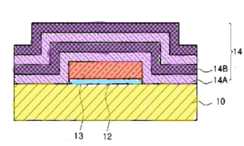
- Reflective metal layer (13, orange in the figure): reflects light generated by the active layer (12), located between the p-layer and the n-layer, and thereby improves light extraction efficiency.
- Barrier layer (14, purple in the figure): prevents diffusion of metal elements from the reflective layer.
- Technical problem: the coefficient of thermal expansion (CTE) of the reflective layer is higher than that of the barrier layer. This creates stress in the reflective layer. At the same temperature, such stress may cause the reflective layer to separate from the active layer or mesa layer, impairing reliability.
- Solution: a stress relief layer is inserted between the reflective layer and the barrier layer. Its CTE lies between the respective CTE values of the two layers and helps buffer thermal stress.
Practical point: This technical background naturally shifts the dispute towards functional limitations, in particular CTE and position, as well as the definition of a “layer”. It is not a simple comparison of material lists. Many claim features in semiconductor, new energy and advanced materials cases rely heavily on functional limitations.
7.2 Disputed issue 1: defining the functional feature — how can a “stress relief layer” be proven?
The “stress relief layer” in the claim was functionally defined through its position, namely between the reflective layer and the barrier layer, and through its property, namely a CTE between those of the adjacent layers. Proving infringement therefore required an indirect functional inference. It was not enough merely to identify material composition or position.
The claimant’s key strategy was to advance a “composite layer” argument. A specific TiNiTiNi sequence was characterised as a composite stress relief layer. Material data were used to infer a composite CTE, with an exemplary calculated value of approximately 11.79 µm/mK. The claimant argued that, at the nanoscale, where each layer was approximately 50–65 nm thick, interlayer interaction caused the structure to operate as a single functional unit. The court accepted this indirect inference, even though the claim did not expressly use the term “composite”.
7.3 Disputed issue 2: design-arounds and functional overlap — can naming something a barrier layer avoid infringement?
Defendants often attempt to avoid literal claim language by modifying the layer stack or by renaming a structural feature. The logic reflected in this case is that functional overlap does not exclude infringement. The legal identity of a layer is determined by its function and effect, as well as by suitability, not by the manufacturer’s chosen terminology.
This is important in practice. Where the claim does not exclude a layer from having multiple functions, a design-around that does not change the functional route may amount only to a structural disturbance, rather than a genuine departure from the scope of protection.
7.4 Disputed issue 3: mapping material characterisation results to claim language
A third challenge was to map high-resolution characterisation data, such as FIB/SEM cross-sectional images, onto legal definitions such as “reflective layer”, “barrier layer” and “stress relief layer”.
The decisive point is not image clarity but mapping logic. Characterisation is only the beginning of the evidence chain. TEM, EDX, SIMS and similar techniques can indicate structure, but expert explanation is required to connect layer interfaces, interdiffusion, thickness and function to the claim features.
The evidence must meet the engineering requirements of UPC practice: representativeness, repeatability and explainability. It must form a chain capable of withstanding challenge.
7.5 Transferable methodology from the case
The most transferable aspect of the case is the sequence in which the case was handled:
construction first → functional reasoning at the outset → evidence collection and testing afterwards → mapping the result into facts that the court can accept.
8 | A practical case-handling checklist
Step 1: Draw a technical map of the disputed issues before drafting submissions
For each claim feature, identify the type of technical dispute involved: structure, function, definition or measurability. At the same time, mark the coupling points between infringement and validity, and identify possible squeeze risks.
Step 2: Turn claim construction into a measurement blueprint
Define the measurement target: what is to be measured, what result would satisfy the claim feature, and how the field of view or sampling range aligns with literal requirements such as plurality or numerical ranges.
Anticipate defence strategies and select the characterisation method accordingly. For example, if the defendant is likely to deny that a composite layer is one layer, the evidence should highlight the mechanism of interaction between thin-film layers.
Step 3: Build the evidentiary funnel and translate the result into court language
The evidence path should run from raw characterisation data, such as electron microscopy images, spectroscopic data and sample cross-sections, to mechanism and material-property reasoning, such as a reasonable derivation of a composite CTE. It should then map each element to the claim features, including plurality and range requirements, and finally express the result as a legal factual conclusion that can be accepted by the court.
Step 4: Perform a squeeze test across validity and infringement
Every key claim construction should immediately be tested in both directions:
- Does this interpretation expand the attack surface for prior art?
- Does this interpretation allow the accused embodiment to escape infringement?
Step 5: Apply an engineering review of evidentiary sufficiency
Use representativeness, repeatability and explainability as internal review criteria. This requires multi-point sampling, validation across multiple chips and traceable sample-preparation procedures.
In semiconductor and materials cases, the evidence chain often depends on interdisciplinary collaboration. In RGTH’s experience, material characterisation and mechanism modelling should be treated as part of the litigation strategy, not as a later supplement. Where appropriate, cooperation with European research institutions, including the Fraunhofer network, can help build a reproducible, defensible and explainable testing and expert evidence system, particularly in the UPC’s highly front-loaded procedural environment.
8.1 | Three typical technical rebuttals and a pre-emptive evidence checklist
The following points translate the above methodology into a litigation-ready evidence design. The key is to anticipate the other side’s most common technical rebuttals and build the response into the evidence strategy from the beginning.
Rebuttal 1: “A composite layer cannot be one layer; atomic-level fusion, such as an alloy, is required.”
Pre-emptive response: Build the explanation chain in advance. The legal identity of a layer should be centred on function and effect, and the context of the specification may distinguish between an alloy and a composite structure. Mechanism evidence should focus on interlayer interaction and mechanical coupling at the nanoscale, showing that several sublayers operate as a single functional unit. The case should not become trapped in the question of whether atomic-level mixing has occurred.
The effective CTE derivation should be presented in a verifiable appendix, including input parameters, calculation and sensitivity analysis.
Rebuttal 2: “You only measured a local area; the result is not representative, not repeatable, or affected by preparation artefacts.”
Pre-emptive response: Use multi-point sampling and verification across multiple chips. Avoid relying on a single image as isolated evidence. The sample preparation procedure should be traceable and auditable, including parameters, batches and contamination control, in order to reduce the attack surface for artefact arguments.
The evidence should be reviewed using the UPC-oriented standard of representativeness, repeatability and explainability.
Rebuttal 3: “Even if the structure exists, the function, such as CTE-based stress relief, has not been proven.”
Pre-emptive response: Translate the functional requirement into a framework based on suitability and mechanism-based reasoning. This avoids being drawn into the uncontrolled terrain of full-life reliability testing.
The reasoning chain should be established first: define the model, boundary conditions and parameters before testing the data. This avoids the logical break that occurs when a model is added only after the measurements have been taken.
The technical narrative should return to thin-film interaction: structure scale, coupling mechanism and derived result should together make the functional limitation concrete.
9 | Conclusion: what is the core competence in semiconductor, new energy and advanced materials litigation?
In semiconductor, new energy and advanced materials litigation, the decisive skill is to create a clear connection between technical analysis and litigation strategy. This requires early identification of disputed issues, a structured evidence path, translation of characterisation results into court language, handling invalidity risks through technical motivation, and avoiding the squeeze effect during the front-loaded stage of the proceedings.
For Chinese companies, this means:
UPC litigation is not a reactive exercise that begins only after a statement of claim is received. It is a systematic project that requires technical and evidentiary preparation in advance.
For further questions and enquiries, please contact: